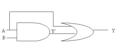
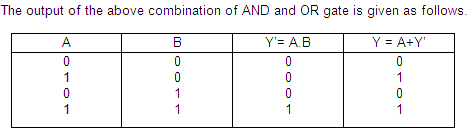
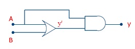
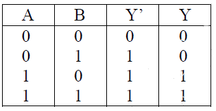
Q1. Write the truth table for the combination of gates shown below
Solution
Q2. Draw a circuit diagram for use of NPN transistor as an amplifier in common emitter configuration. The input resistance of a transistor is 1000 Ω. On changing its base current bv 10 uA. the collector current increases bv 2 mA.
If a load resistance of 5 k Ω is used in the circuit, calculate:
(i) The current gain
(ii) Voltage gain of the amplifier
Solution
 Numerical: Given
Rin = 1000 Ω
Δ IB = 10 μA = 10-5 A
ΔIC = 2mA = 2 x 10⁻³A
Rout = 5 kΩ = 5 x 10³ Ω
(i) Current gain
Numerical: Given
Rin = 1000 Ω
Δ IB = 10 μA = 10-5 A
ΔIC = 2mA = 2 x 10⁻³A
Rout = 5 kΩ = 5 x 10³ Ω
(i) Current gain
 (ii) Voltage gain

Q3. Name the p-n junction diode which emits spontaneous radiations when forward biased. How do we choose the semiconductor, to be used in these diodes, if the emitted radiation is to be in the visible region?
Solution
The p-n junction diode, which emits spontaneous radiation when forward biased, is known as the light emitting diode or LED.
The visible light is from 0.45 µm to 0.7 µm and corresponding energy is between 2.8eV to 1.8 eV . therefore, the least band gap of the semiconductor to be used in LED , in order to have the emitted radiation to be in the visible region, should be 1.8 eV . Phosphorus doped gallium arsenide and gallium Phosphide are two such semiconductors.
Q4. State briefly the underlying principle of transistor oscillator. Draw a circuit diagram showing how the feed back is accomplished by inductive capacitance. Explain the oscillator action.
Solution
A transistor as an oscillator:
The circuit of a tuned collector in CE configuration is shown in fig.
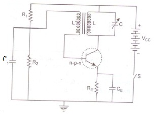 The circuit contains a tuned circuit made of variable capacitor C and an inductor L in the collector circuit and hence is named as tuned collector oscillator
The feed back coil L' connected to base circuit is mutually coupled with coil L (due to phenomenon of mutual induction ); the mutual inductance of L and L' being M. In practice L and L' form the primary and secondary coil of the transformer
The biasing is provided by emitter resistance RE and potential divider arrangement consisting of resistances R1 and R2. The capacitor C1 connected in the base circuit provides low reactance path to the oscillations and the capacitor CE is the emitter by-pass capacitor so that the resistor RE has no effect on the ac operation of the circuit.
Circuit Operation:
When the collector supply voltage is switched on by closing switch S, collector current starts increasing and the capacitor C is charged. When the capacitor attains maximum charge it discharges through coil L, setting up oscillations of natural frequency
The circuit contains a tuned circuit made of variable capacitor C and an inductor L in the collector circuit and hence is named as tuned collector oscillator
The feed back coil L' connected to base circuit is mutually coupled with coil L (due to phenomenon of mutual induction ); the mutual inductance of L and L' being M. In practice L and L' form the primary and secondary coil of the transformer
The biasing is provided by emitter resistance RE and potential divider arrangement consisting of resistances R1 and R2. The capacitor C1 connected in the base circuit provides low reactance path to the oscillations and the capacitor CE is the emitter by-pass capacitor so that the resistor RE has no effect on the ac operation of the circuit.
Circuit Operation:
When the collector supply voltage is switched on by closing switch S, collector current starts increasing and the capacitor C is charged. When the capacitor attains maximum charge it discharges through coil L, setting up oscillations of natural frequency
 These oscillations induce a small voltage in coil L' by mutual induction. This induced voltage is the feed back voltage, its frequency is same as that of resonant LC circuit but its magnitude depends on the number of turns in L' and coupling between L and L' The feedback voltage is applied between the base and emitter and appears in the amplified form in the collector circuit. A part of this amplifier energy is used to meet losses taking place in oscillatory circuit to maintain oscillations in tank circuit and the balance is radiated out in the form of electromagnetic waves.
Positive Feed Back-
The feed back applied in tuned collector oscillator circuit is positive. This may be seen as follows : A phase shift of 180º is created between the voltage of L and L' due to transformer action. A further phase shift of 180º arises between base emitter and collector circuit due to transistor action in CE configuration. Thus the net phase becomes 360º (or zero) which is the required condition for a positive feed back. Due to positive feed back the energy fed back to the tank circuit is in phase with the generated oscillations, thus maintaining oscillations.
These oscillations induce a small voltage in coil L' by mutual induction. This induced voltage is the feed back voltage, its frequency is same as that of resonant LC circuit but its magnitude depends on the number of turns in L' and coupling between L and L' The feedback voltage is applied between the base and emitter and appears in the amplified form in the collector circuit. A part of this amplifier energy is used to meet losses taking place in oscillatory circuit to maintain oscillations in tank circuit and the balance is radiated out in the form of electromagnetic waves.
Positive Feed Back-
The feed back applied in tuned collector oscillator circuit is positive. This may be seen as follows : A phase shift of 180º is created between the voltage of L and L' due to transformer action. A further phase shift of 180º arises between base emitter and collector circuit due to transistor action in CE configuration. Thus the net phase becomes 360º (or zero) which is the required condition for a positive feed back. Due to positive feed back the energy fed back to the tank circuit is in phase with the generated oscillations, thus maintaining oscillations.
The circuit contains a tuned circuit made of variable capacitor C and an inductor L in the collector circuit and hence is named as tuned collector oscillator
The feed back coil L' connected to base circuit is mutually coupled with coil L (due to phenomenon of mutual induction ); the mutual inductance of L and L' being M. In practice L and L' form the primary and secondary coil of the transformer
The biasing is provided by emitter resistance RE and potential divider arrangement consisting of resistances R1 and R2. The capacitor C1 connected in the base circuit provides low reactance path to the oscillations and the capacitor CE is the emitter by-pass capacitor so that the resistor RE has no effect on the ac operation of the circuit.
Circuit Operation:
When the collector supply voltage is switched on by closing switch S, collector current starts increasing and the capacitor C is charged. When the capacitor attains maximum charge it discharges through coil L, setting up oscillations of natural frequency
Q5. In the given figure, is (i) The emitter (ii) collector forward or reverse biased? Justify. 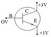
Solution
Figure shows n-p-n transistor(i) Emitter is reversed biased because n-region is connected to higher potential.(ii) Collector is also reversed biased because n-region of p-n junction is at higher potential than p-region.
Q6. Distinguish between photo current and dark current.
Solution
When light of certain frequency reaches the p-n junction and if the energy of the photon is greater than the gap energy, the photon entering the junction breaks the covalent bond and produce electron -hole pair.The resulting current is called the photo current.
When there is no light the reverse saturation current flowing is called dark current.
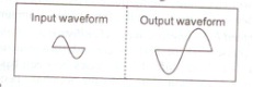
Q7. Draw the circuit diagram of a common-emitter amplifier using an n-p-n transistor. What is the phase difference between the input signal and output voltage ? Draw the input and output wave forms of the signal. Write the expression for its voltage gain. State two reasons why a common emitter amplifier is preferred to a common base amplifier
Solution
The circuit of a common-emitter amplifier using an n-p-n transistor is shown below :
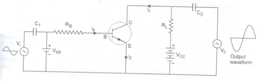 In a common emitter amplifier circuit, the input signal voltage and output collector voltage are in opposite phase. i.e 180° out of phase. Thus the phase difference between the input signal and output voltage is 180°.
The input and output wave forms are shown in fig.
In a common emitter amplifier circuit, the input signal voltage and output collector voltage are in opposite phase. i.e 180° out of phase. Thus the phase difference between the input signal and output voltage is 180°.
The input and output wave forms are shown in fig.
 where β is the current gain , RL the load resistance and Ri the input resistance.
Reasons for using a common emitter amplifier over common base amplifier:
(i) Voltage gain is quite high without any phase change of signal voltage.
(ii) Voltage gain is uniform over a wide frequency range or power gain is high .
where β is the current gain , RL the load resistance and Ri the input resistance.
Reasons for using a common emitter amplifier over common base amplifier:
(i) Voltage gain is quite high without any phase change of signal voltage.
(ii) Voltage gain is uniform over a wide frequency range or power gain is high .
In a common emitter amplifier circuit, the input signal voltage and output collector voltage are in opposite phase. i.e 180° out of phase. Thus the phase difference between the input signal and output voltage is 180°.
The input and output wave forms are shown in fig.
where β is the current gain , RL the load resistance and Ri the input resistance.
Reasons for using a common emitter amplifier over common base amplifier:
(i) Voltage gain is quite high without any phase change of signal voltage.
(ii) Voltage gain is uniform over a wide frequency range or power gain is high .
Q8. Which of the one between silicon and germanium preferred in the manufacturing of semiconductor devices? Why?
Solution
Silicon is preferred to germanium in the manufacture of semiconductor devices (e.g. semiconductor diode, transistor, etc.) due to the following reasons:-
(i) The leakage current in silicon is very small as compared to that of germanium.
(ii) The working temperature of silicon is more than that of germanium. The structure of germanium will be destroyed at a temperature of about 1000C. However silicon can be operated up to about 2000C.
Q9. What do you mean by depletion layer and potential barrier for a p-n junction.
Solution
Depletion layer is the region created around the p-n junction which is devoid of free charge carriers and has immobile ions.It is created due to diffusion of majority carriers across the junction when p-n junction is formed.
Potential barrier is the potential difference or junction voltage developed across the junction due to migration of majority charge carriers across it when p-n junction is formed. It opposes further migration of majority carriers across the junction due to this junction voltage.
Q10. Why do hole carriers present in n-type semiconductor?
Solution
Due to the addition of pentavalent impurity, n-type material has a large number of free electrons. However, even at room temperature, some of the covalent bond breaks, thus releasing an equal number of free electrons and holes. Therefore n-type material has a large number of free electrons and a small number of holes.
Q11. How does the width of the depletion region of a p-n junction vary, if the reverse bias applied to it decrease ?
Solution
If the reverse bias decreases,the width of depletion region of the p-n junction decreases.
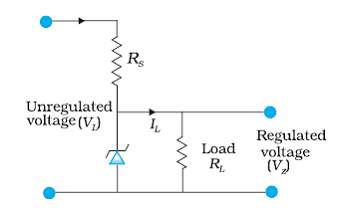
Q12. The output of an unregulated d.c power is to be regulated. Name the device that can be used for this purpose and draw the relevant circuit diagram.
Solution
A Zener diode is used as a voltage regulator. The circuit arrangement consists of RS a suitable resistance joined in series of input unregulated voltage Vi so as to control current flowing through Zener with in a safe limit. RL is a load resistor across which regulated output voltage VZ is obtained.
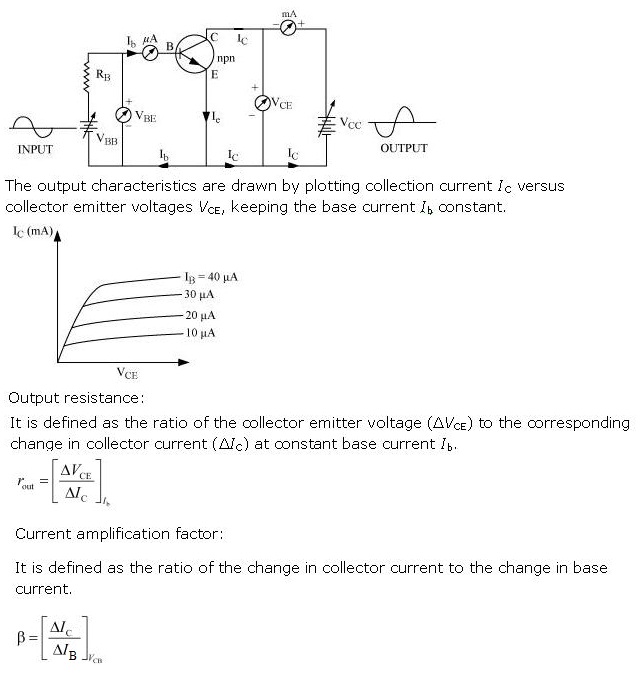
Q13. For an n-p-n transistor in the common-emitter configuration, draw a labelled circuit diagram of an arrangement for measuring the collector current as a function of collector-emitter voltage for at least two different values of base current. Draw the shape of the curves obtained. Define the terms:(i) output resistance and (ii) 'current amplification factor'.
Solution
Q14. What is a zener diode? why is it also known as breakdown diode.Name one application of Zener diode.
Solution
A zener diode is a properly doped p-n junction diode, which has a sharp breakdown voltage.It is always reverse-biased.It works in the breakdown region of the characteristics, so it is also called breakdown diode.It is used for voltage regulation in electronic power supply.
Q15. What is meant by the term doping of an intrinsic semiconductor ? How does it affect the conductivity of a semiconductor ?
Solution
Doping of an Intrinsic Semiconductor : The mixing of a small amount of pentavalent (e.g., phosphorus) or trivalent (e.g., aluminium) substance as impurity in a pure semiconductor (e.g., Ge, Si) is called doping.
Doping increases the conductivity of a semiconductor.
Q16. Show the output waveforms (Y) for the following inputs A and B of
(i) OR gate (ii) NAND gate

Solution
Given input signals:
 Output of an OR gate:
 For OR gate, Output = A + B
Between t1 and t2:
A = 0,B = 0, Output = 0 + 0 = 0
Between t2 and t3:
A = 1,B = 0, Output = 1 + 0 = 1
Between t3 and t4:
A = 1,B = 1, Output = 1 + 1 = 1
Between t4 and t5:
A = 0,B = 1, Output = 0 + 1 = 1
Between t5 and t6:
A = 0,B = 0, Output = 0 + 0 = 0
Between t6 and t7:
A = 1,B = 0, Output = 1 + 0 = 1
Between t7 and t8:
A = 0,B = 1, Output = 0 + 1 = 1
Output of an NAND gate:
For OR gate, Output = A + B
Between t1 and t2:
A = 0,B = 0, Output = 0 + 0 = 0
Between t2 and t3:
A = 1,B = 0, Output = 1 + 0 = 1
Between t3 and t4:
A = 1,B = 1, Output = 1 + 1 = 1
Between t4 and t5:
A = 0,B = 1, Output = 0 + 1 = 1
Between t5 and t6:
A = 0,B = 0, Output = 0 + 0 = 0
Between t6 and t7:
A = 1,B = 0, Output = 1 + 0 = 1
Between t7 and t8:
A = 0,B = 1, Output = 0 + 1 = 1
Output of an NAND gate:
 For NAND gate:
Output =
For NAND gate:
Output =  Between t1 and t2:
A = 0,B = 0, Output =
Between t1 and t2:
A = 0,B = 0, Output =  = 1
Between t2 and t3:
A = 1,B = 0, Output =
= 1
Between t2 and t3:
A = 1,B = 0, Output =  = 1
Between t3 and t4:
A = 1,B = 1, Output =
= 1
Between t3 and t4:
A = 1,B = 1, Output =  = 0
Between t4 and t5:
A = 0,B = 1, Output =
= 0
Between t4 and t5:
A = 0,B = 1, Output =  = 1
Between t5 and t6:
A = 0,B = 0, Output = = 1
Between t6 and t7:
A = 1,B = 0, Output = = 1
Between t7 and t8:
A = 0,B = 1, Output = = 1
= 1
Between t5 and t6:
A = 0,B = 0, Output = = 1
Between t6 and t7:
A = 1,B = 0, Output = = 1
Between t7 and t8:
A = 0,B = 1, Output = = 1
Output of an OR gate:
For OR gate, Output = A + B
Between t1 and t2:
A = 0,B = 0, Output = 0 + 0 = 0
Between t2 and t3:
A = 1,B = 0, Output = 1 + 0 = 1
Between t3 and t4:
A = 1,B = 1, Output = 1 + 1 = 1
Between t4 and t5:
A = 0,B = 1, Output = 0 + 1 = 1
Between t5 and t6:
A = 0,B = 0, Output = 0 + 0 = 0
Between t6 and t7:
A = 1,B = 0, Output = 1 + 0 = 1
Between t7 and t8:
A = 0,B = 1, Output = 0 + 1 = 1
Output of an NAND gate:
For NAND gate:
Output =
Between t1 and t2:
A = 0,B = 0, Output = = 1
Between t2 and t3:
A = 1,B = 0, Output = = 1
Between t3 and t4:
A = 1,B = 1, Output = = 0
Between t4 and t5:
A = 0,B = 1, Output = = 1
Between t5 and t6:
A = 0,B = 0, Output = = 1
Between t6 and t7:
A = 1,B = 0, Output = = 1
Between t7 and t8:
A = 0,B = 1, Output = = 1
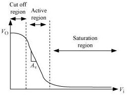
Q17. Illustrate the cut off, active, and saturation regions on a plot of V0 and Vi for a transistor switch circuit.
Solution
Q18. Can we measure the potential difference of a p-n junction by putting a sensitive voltmeter across its terminals?
Solution
No, because there are no free charge carriers in the depletion region .In the absence of any forward biasing it offers infinite resistance.
Q19. Give the barrier potential of :
silicon
germanium
Solution
The barrier potential for
silicon : 0.7 V
germanium : 0.3 V
Q20. Differentiate between Half-wave rectifier and full- wave rectifier
Solution
Half-wave rectifier
Full-wave rectifier
1. The output voltage is unidirectional, intermittent and varying in magnitude.
1. The output voltage is unidirectional, continuous and varying in magnitude.
2. The frequency of output signal is same as that of input signal.
The frequency of output signal is double as that of input signal.
Q21. Why are germanium and silicon preferred to other semiconductors in solid state devices?
Solution
It is because the energy required to break their covalent bonds is small. (Being 0.7eV for germanium and 1.1eV for silicon.
Q22. Why is the amount of impurity added to a pure semiconductor closely controlled?
Solution
Doping a pure semiconductor can have quite marked effect on the conductivity of the material. The addition of one impurity atom in one hundred million will increase the conductivity by 11 times at room temperature. Therefore the amount of impurity added has to be closely controlled during the preparation of the extrinsic semiconductor.
Q23. Write the truth table for the following combination of gates?

Solution
 The Boolean expression for the given combination can be written as:
y' =A+B
y = A.y'
The truth table for the given combination is :
The Boolean expression for the given combination can be written as:
y' =A+B
y = A.y'
The truth table for the given combination is :
Q24. Draw the I-V characteristics of a solar cell.
Solution

Q25. Calculate emitter current for which β = 100 IB = 20μA?
Solution
β = 100,
IB = 20μA = 20 x 10-6 A
β =  IC = β IB = 100 x 20 = 2000μA
Using IE =IB + IC
IE = 20 x 10-6 + 2000μA
IE = 2020μA
IC = β IB = 100 x 20 = 2000μA
Using IE =IB + IC
IE = 20 x 10-6 + 2000μA
IE = 2020μA
IC = β IB = 100 x 20 = 2000μA
Using IE =IB + IC
IE = 20 x 10-6 + 2000μA
IE = 2020μA
Q26. Name the gate obtained from the combination of gates shown in the figure. Draw its logic symbol. Write the truth table of the combination.
Solution
NOR gate is obtained by the combination of gates shown.
Its logic symbol is :
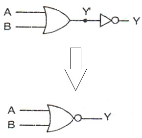 Logical symbol of NOR gate
Boolean expression of NOR gate is
Logical symbol of NOR gate
Boolean expression of NOR gate is  Input
Output
A
B
0
0
1
1
0
1
0
1
1
0
0
0
Input
Output
A
B
0
0
1
1
0
1
0
1
1
0
0
0
Logical symbol of NOR gate
Boolean expression of NOR gate is
Input
Output
A
B
0
0
1
1
0
1
0
1
1
0
0
0
Q27. a) The adjoining figure shows the V-I characteristic of a semiconductor diode :
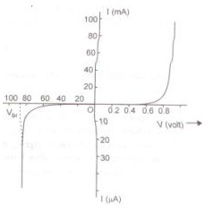 (i) Identify the semiconductor diode used.
(ii) Draw the circuit diagram to obtain the given characteristics of this diode.
(iii) Briefly explain how this diode can be used as a voltage regulator.
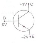
b) In the fig. given along side is (i) the emitter and (ii) the collector forward or reverse biased ?
(i) Identify the semiconductor diode used.
(ii) Draw the circuit diagram to obtain the given characteristics of this diode.
(iii) Briefly explain how this diode can be used as a voltage regulator.
b) In the fig. given along side is (i) the emitter and (ii) the collector forward or reverse biased ?
(i) Identify the semiconductor diode used.
(ii) Draw the circuit diagram to obtain the given characteristics of this diode.
(iii) Briefly explain how this diode can be used as a voltage regulator.
b) In the fig. given along side is (i) the emitter and (ii) the collector forward or reverse biased ?
Solution
a)
(i) Semiconductor diode used is zener diode (but the voltage quoted in fig. are much less than actual values. Vbr is usually < 6 V)
(ii) The circuit diagram for reverse characteristics of Zener diode is shown fig.
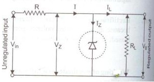 (iii) Zener diode as a voltage Regulator:
In the reverse breakdown region, the voltage across the zener diode remains constant, even if the current through zener diode increases considerably. The circuit diagram for a zener diode as voltage regulator is shown above. Here the zener diode is joined in reverse bias to the fluctuating d.c input voltage through resistance R of suitable value depending upon the zener voltage.The constant output is taken across a load resistance RL connected in parallel with zener diode.
When the input d.c voltage increases beyond a certain limit, the voltage across the zener diode becomes constant equal to zener break down voltage , but the current through the zener diode circuit rises sharply as the dynamic resistance of zener diode becomes almost zero, after zener breakdown voltage.Due to which there is an increase in voltage drop across R. Since RL is connected in parallel so the voltage across RL remains the same as that of zener break down voltage.Hence the output voltage remains constant.
b)The given transistor is p-n-p transistor. The emitter is reverse biased and the collector is forward biased.
(iii) Zener diode as a voltage Regulator:
In the reverse breakdown region, the voltage across the zener diode remains constant, even if the current through zener diode increases considerably. The circuit diagram for a zener diode as voltage regulator is shown above. Here the zener diode is joined in reverse bias to the fluctuating d.c input voltage through resistance R of suitable value depending upon the zener voltage.The constant output is taken across a load resistance RL connected in parallel with zener diode.
When the input d.c voltage increases beyond a certain limit, the voltage across the zener diode becomes constant equal to zener break down voltage , but the current through the zener diode circuit rises sharply as the dynamic resistance of zener diode becomes almost zero, after zener breakdown voltage.Due to which there is an increase in voltage drop across R. Since RL is connected in parallel so the voltage across RL remains the same as that of zener break down voltage.Hence the output voltage remains constant.
b)The given transistor is p-n-p transistor. The emitter is reverse biased and the collector is forward biased.
Comments
Post a Comment